


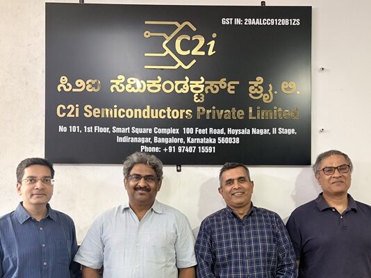

An Indian startup is redesigning power for AI servers, cutting energy losses, boosting GPU performance, and building chips that could shape the next generation of global AI infrastructure. In a conversation with Preetam Tadeparthy and Vikram Gakhar of C2i Semiconductor, Nidhi Agarwal and Saba Aafreen from EFY explore the technology, challenges, and vision behind these innovations.
Q. What inspired you to start C2i Semiconductors and focus on AI power solutions?
A. Our journey began in 2024 when we started exploring the problem we truly wanted to solve. Stepping away from the influence and professional certainty of our global roles was a significant choice, driven by the mission to build a global technical authority for energy-efficient AI infrastructure and address the industry’s most critical power challenges.
We questioned whether the ecosystem could support a global technology venture. After months of reflection, we decided to build benchmark technology from India, led by Indian talent, for the global market. We evaluated areas such as motor control, industrial automation, and enterprise solutions before identifying enterprise AI power as the next frontier.
Power for AI is a trillion-dollar opportunity with complex technical challenges, and solving it from India could create a strong foundation for future expansion. This clarity led us to form C2i Semiconductors, raise our first round of funding, and begin developing technology aimed at shaping the future of AI power globally.
Power for AI and data centre applications presents a complex challenge, alongside a clear intent to establish a strong benchmark for semiconductor start-ups in India.
Q. What role does C2i Semiconductors play in powering next-generation AI infrastructure?
A. C2i Semiconductors stands for conversion, control, and intelligence, which define the company’s approach to power electronics. Conversion transforms electrical power between voltage domains, control regulates this process to ensure stability and efficiency, and intelligence enhances power management through embedded capabilities in controllers or AI systems.
Building on this foundation, the company is developing a total power solution for AI infrastructure, particularly hyperscalers and data centres, covering the entire grid-to-core power delivery chain. This includes converting high-voltage input from the grid, typically 400 to 800 volts, into tightly regulated power suitable for advanced processors.
The company aims to build a product-driven technology firm from India that re-architects end-to-end power delivery for server platforms while setting new global benchmarks in innovation and quality.
Q. What products are you currently developing, and when are they expected to reach the market?
A. C2i Semiconductors’ first-generation chips are approaching tape-out, scheduled for 3Q ’26. The company is building a grid-to-core power architecture for AI systems, which involves multiple stages of power conversion.
The first generation focuses on the final stage of processor power delivery, developing controllers and power solutions for GPUs and high-performance processors. These convert intermediate bus voltages of about 4 to 16 volts into precise core voltages, while delivering currents of up to 4kA with millivolt-level regulation and high efficiency.
Q. What technical challenges has C2i Semiconductors faced in converting high-voltage input to sub-1-volt rails for AI processors?
A. Our first-generation product does not directly convert 800 volts to sub-1-volt rails. The current industry standard, covering about 90 per cent of the market, uses a three-stage conversion from 400 volts to 48 volts, then to 12 or 6 volts, and finally to the GPU core voltage.
Our current product, taping out in 3Q ’26, focuses on this final stage. For next-generation designs, we are exploring direct 800-volt to bus voltage conversion and evaluating whether a one- or two-stage final conversion is more efficient.
A key challenge is the topology that enables such large conversion ratios (~1000:1) in one step and identifying a control approach that balances efficiency with load demand at the GPU end.
C2i’s architecture’s uniqueness lies in its software-defined VR approach. For low-voltage stages, silicon is sufficient, but for high-voltage conversion, we partner with fabs that provide GaN solutions.
Q. How does C2i Semiconductors manage switching losses at extreme conversion ratios?
A. Our smart power stages incorporate proprietary IP that optimises how we switch FETs, which significantly reduces switching losses. This IP gives us a performance advantage over competitors, based on the data we have collected, and a large portion of the efficiency improvement in our system comes directly from these optimised switching techniques.
Q. At what level is the 10% efficiency gain measured and where does it come from?
A. The 10 per cent efficiency gain is measured at the system level and comes from the company’s proprietary IP, with a reduced number of stages and improvements in both control and power conversion at each stage.
The company has filed 9 patents, and several more are in progress, enabling extremely fast switching and highly optimised power conversion.
Efficiency losses in a system typically occur in three areas. First, during voltage conversion from grid level to core level, each step incurs losses. Second, the intermediate bus routing on the motherboard, carrying hundreds to thousands of amps, introduces resistive losses. Third, GPU operation involves frequent transitions between high-performance and deep sleep modes, where latency in power management can reduce performance (indirect efficiency).
The company’s IP optimises across all three levels, resulting in a net 10 per cent gain in queries processed per watt.
Q. How would you sum up the advantages of your power management solutions?
A. Our power management architecture offers several differentiators over incumbent solutions. We are developing a software-defined voltage regulator that is highly scalable, operating from grid-to-core, and is processor-agnostic, capable of supporting systems from 100 watts to several kilowatts without compromising performance.
Key technical advantages include superior thermal efficiency, higher overall system efficiency, and compact density, reducing footprint requirements.
Additionally, the company’s proprietary IP extends the lifespan of power solutions, effectively doubling the life of server power systems compared to existing components. These innovations translate into measurable benefits for AI infrastructure, including up to a 10 per cent increase in GPU performance, measured as tokens processed per watt, and significantly longer server lifecycles, allowing refurbishment and extended operation without power limitations becoming a bottleneck.
Q. How does your power solution compare to traditional server voltage regulators?
A. Our first-generation products work with existing voltage regulator systems, so they remain compatible with current setups. However, the key differentiation is scalability.
Data centres require solutions that can support anything from about 100 amps to several kilowatts, depending on the processor and workload. Our architecture allows a single validated product to scale from a few hundred watts to tens of kilowatts, reducing setup time and improving uptime.
We are also developing algorithms and technologies for near-zero setup time and minimal downtime through plug-and-play, self-tuning solutions with strong diagnostics. Although individual component gains may appear incremental, their combined impact delivers substantial system-level improvements.
Q. How does the C2i Semiconductors’ solution integrate with rack- or cluster-level power management?
A. C2i is focused on sequentially building and validating our core products, primarily at the motherboard level. While we are releasing multiple products in parallel to accelerate development, full rack- or cluster-level integration is not feasible today due to resource constraints.
Looking ahead to 2027, once we have a robust 800-volt to intermediate bus conversion and controllers capable of handling sidecar power, we plan to partner with other players to extend our solutions to rack- and cluster-level power management.
The toughest challenge before tape-out has been optimising power switching to extract maximum performance from our IP, which is capable of double-digit gains, without compromising silicon quality or reliability. At this stage, it is a careful balance between performance and robustness.
At C2i, we prioritise quality, even if it costs a fraction of a per cent in performance, ensuring plug-and-play operation with minimal downtime. This is critical because the power module is mission-critical for AI and GPU workloads, and any quality issue directly impacts system performance. Our focus remains on delivering a precise and robust solution that consistently meets processor requirements, even at a marginal trade-off in peak performance.
Q. When was the company founded?
A. C2i Semiconductors was established in early 2024 by a founding team of senior power architects. We leverage over 60 years of combined global expertise to architect specialised ‘Grid-to-GPU’ power systems, bringing a mature, expert-led approach to solving critical energy challenges in the AI infrastructure space.
Q. How do you approach co-design between power delivery and AI compute loads?
A. Co-design involves two layers. For power delivery, we work closely with processor companies and OEMs because every server solution has unique requirements. This collaboration ensures our technology meets the exact needs of each application.
For hardware–software partitioning, our die currently runs only C2i Semi’s own algorithms, both in hardware and software. We collaborate with customers to demonstrate these algorithms’ performance advantages. If a feature meaningfully improves system performance, we enable it, allowing customers to benefit and potentially market it.
Internal hardware–software partitioning is guided by architectural decisions and continuously refined through customer engagement.
Q. How close is C2i Semiconductors to the physical limits of power density?
A. Based on the process technologies currently available to C2i, the products planned for 2027 will be approaching the physical limits of power density. While future advances in process technology could push these limits further, we are already pushing our current design vectors to their maximum potential.
Q. What is the integration level and key challenge of your first power module?
A. The first-generation module approaching tape-out separates control and power into two chips. The next iteration later this year will move to a one-and-a-half-chip design, followed early next year by a fully integrated single-chip module that can plug in and scale to any power requirement.
Q. How did you validate the reliability of your design before committing to silicon?
A. We validate reliability through close collaboration with fabs such as Tower and GlobalFoundries, reviewing designs and data with their process engineers on a fortnightly basis.
Beyond that, C2i’s experience gives us an edge. Our team has worked on similar products long enough to anticipate critical gaps that simulations cannot fully capture. For areas that cannot be validated pre-silicon, we plan accordingly, ensuring budgets and design margins account for variations between silicon and simulation.
This careful planning addresses one of the toughest challenges in engineering high-performance, reliable power solutions.
Q. What are the main risks between tape-out and first silicon validation?
A. The biggest risk is schedule, especially since we are on a multi-project wafer. Any slip in timing can delay silicon delivery, so we focus on completing all tasks on target while leaving time to verify changes.
Another challenge is the inherent uncertainty between simulation and silicon. Beyond the chip itself, factors such as packaging, package-to-motherboard interactions, and passive components introduce variations that are difficult to model accurately.
No one can guarantee 100 per cent performance at this stage, so we build in design and verification buffers to mitigate these risks and ensure the final product meets expectations.
Q. What EDA flows did you use for analogue and mixed-signal verification?
A. For analogue and mixed-signal verification, we primarily use the standard Cadence flow, including back-end processes. Cadence has been extremely supportive, and we also leverage Synopsys and Siemens tools, which have been highly supportive of C2i Semi.
The reason for using multiple EDA flows is to ensure silicon quality and capture the gap between simulation and reality. Different tools handle parasitic extraction and package interactions differently, so cross-checking across tools highlights variations and helps us optimise the design.
This multi-tool approach, combined with fab-required back-end PD checks, ensures a thorough and robust verification process.
Q. What is the company’s packaging strategy for high-intensity power modules?
A. We are working with two experienced partners who have deep expertise in high-performance power packaging. Their knowledge ensures that both our first- and second-generation products are well supported in terms of packaging and process, allowing us to reliably handle high-intensity power requirements.
Q. How does a start-up like C2i Semiconductors protect its core IP while collaborating with customers or partners?
A. We protect our core technology primarily through patents. We have already filed nine and have several more in the pipeline. For collaborations, whether with universities or partners, any IP developed under a C2i project belongs to the company, with clear agreements in place for the use of any third-party IP.
For OEMs and other customers, we treat them as clients, sharing differentiated features and performance as needed while ensuring our core IP remains fully protected.
Q. Who are your target customers, and how do you position in India and globally?
A. The company’s primary customers are global data centre operators, AI players, hyperscalers, network companies, and storage providers. We are actively engaging with all of them, demonstrating our silicon capabilities and receiving positive feedback on our feature set and performance targets.
In India, leading customers are evolving into self-sufficient OEMs by building servers and systems in-house, unlocking new pathways for indigenous product technologies.
India is transitioning from deploying AI infrastructure to manufacturing it domestically. As Indian players start building population-scale AI solutions, they will adopt more system engineering practices, creating semiconductor opportunities.
By establishing success in the global market first, the company aims to enter the Indian ecosystem in a structured and sustainable manner.
While the government is developing initiatives under ISM 2.0 and ISM 3.0 to support domestic OEM and ODM capabilities, there are currently no dedicated programmes ensuring semiconductor products developed in India are consumed locally.
Q. How does the company approach partnerships with OEMs, AI companies, or start-ups to scale the business?
A. Partnerships begin the moment the silicon is available, as performance metrics speak for themselves. We present our first-generation silicon to OEMs, ODMs, processor players, and other technology partners, demonstrating both current capabilities and a clear roadmap for future generations, while showing production readiness for volume.
Gen 1 establishes thermal, performance, and reliability benchmarks, while Gen 2 and 3 demonstrate how these metrics improve, building confidence in long-term collaboration.
Over time, we work closely with fabs, packaging vendors, and system integrators to define new process nodes, package technologies, and thermal solutions. This multi-generation roadmap and end-to-end approach, rare even among large incumbents, form the foundation for strategic partnerships and long-term scaling, all driven from India by our start-up team.
Q. How is C2i Semiconductors funded, and how will you monetise the upcoming tape-outs and future chip designs?
A. The company has raised $19 million across two funding rounds from seasoned investors, including Ganapathy Subramaniam, Lip-Bu Tan, and Peak XV, representing one of the largest VC raises for a semiconductor start-up in India.
The funds are mainly being used to tape-out the first-generation two-chip solution, covering fabrication, development, testing, and R&D for next-generation products.
Part of the investment is also going towards building back-end, systems, and applications, teams outside India, particularly in the US and Taiwan, to support customers closely. Since these products are complex and mission-critical, they require strong technical engagement.
The monetisation strategy is based on delivering high-performance power management solutions for AI infrastructure while building an intelligent grid-to-GPU power architecture.
Q. Can you share your revenue model and whether the company is profitable yet?
A. At this stage, we have not generated revenue, as our products are still in the development phase. Our first chips are expected to tape-out this year, and revenue will begin once they are adopted by customers in the market.
We expect meaningful revenue traction to begin around late next year and grow further towards 2028.
Q. Are you also receiving any funding support from the government?
A. Yes, we are a DLI-approved organisation and receive support under the DLI 1.0 scheme. With the recent announcement of ISM 2.0, we also plan to work closely with the government to explore further support under the new framework.
Q. Where is your manufacturing carried out: in-house or outsourced?
A. Our manufacturing is currently outsourced. Fabrication is carried out through foundries such as GlobalFoundries and Tower, which are located outside India. At present, the required process technologies are not yet available within India.
Similarly, packaging is also handled internationally, primarily in locations such as Singapore, the US, and the China ecosystem.
Q. What is your roadmap for entering new markets and geographies as a start-up?
A. Our focus is global from day one, targeting North America, Europe, China, and Taiwan. The priority is to establish C2i Semi as a trusted technology player with differentiated, high-quality enterprise products.
Once that foundation is set, we plan to expand into adjacent markets such as motor control, industrial automation, and edge AI applications in automotive, telecom, and other sectors. For the next two to four years, however, our full attention remains on delivering first-class enterprise solutions without distractions.
Q. Are you looking for tie-ups with academia?
A. Yes, we have MOUs and ongoing projects with IIT Kharagpur and IISc Bangalore for next-generation R&D. Internationally, we are also collaborating with Tyndall National Institute in Cork, Ireland. These partnerships help advance our upcoming solutions.
Q. Are you looking to add new channel partners or distributors, and what would be the ideal profile?
A. Yes, we need partners who can work closely with our customers and support our technology requirements. Once we reach production, we will engage value-added distributors who can not only handle volume production but also provide application and technical support.
We are looking at partners in regions such as Taiwan, China, and East Asia, and will bring them on board at the appropriate stage.
Q. What are the main challenges you are addressing to scale quickly as a start-up?
A. One key challenge is building the back-end flow, handling post-silicon tape-out, testing, validation, qualification, and ramping to production volumes.
We are also growing systems and applications teams to work closely with customers, understand their requirements, and tune our products accordingly. This scaling is non-linear, as we plan to hire significantly over the next few quarters.
Q. What challenges have you faced in scaling operations, hiring talent, and balancing R&D with commercialisation?
A. India has strong generic talent, but finding engineers with domain expertise in high-power AI applications and alignment with the company’s mission has been a major challenge. Competing with large corporations for experienced talent requires patience and careful selection.
We were fortunate to build a strong founding team that later helped develop the next layer of leadership. Motivating people to balance short-term stability with long-term impact is also critical.
Another challenge is keeping pace with a rapidly evolving AI market while building a multi-year technology roadmap from India. Much of this requires vision and informed judgement about where the market is heading.
As India’s ecosystem grows towards ‘Make in India’ AI infrastructure, both talent availability and market access should improve.
Q. What are your plans for future growth, and where are you investing most right now?
A. Our future growth focuses on three areas. First, completing the tape-out, manufacturing, testing, and qualification of our products, which is capital-intensive. Second, investing in R&D for next-generation products to push technology limits. Third, building and expanding teams to support these efforts.
Q. What is your vision for a ‘Make in India’ AI ecosystem in the future?
A. Our vision is to enable population-scale AI that is affordable and optimised for India’s needs. Today, AI infrastructure is expensive, but solutions built in India for India can reduce costs and improve accessibility while ensuring long-term efficiency and reliability.
We also expect India to adopt a more distributed and edge-centric AI model, supporting applications such as speech, image, and local language AI on optimised infrastructure.
As the ecosystem evolves, more system-level design and semiconductor innovation will emerge from India, shifting the focus from ‘assembled in India’ to ‘architected in India.’

