
Paras Semiconductor will get access to BroadPak’s specialised technology expertise
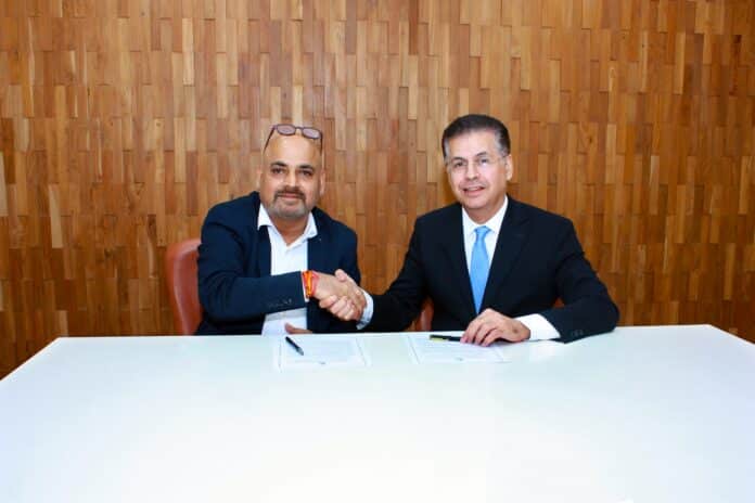
Paras Semiconductor has recently announced a partnership with US-based BroadPak Corporation. The company aims to establish a well equipped Outsourced Semiconductor Assembly and Test (OSAT) facility in the country with advanced heterogeneous integration and 3D packaging capabilities.
The new facility will offer chiplet integration facilities, 2.5D/3D packaging, hybrid bonding, wafer-level and panel-level fan-out packaging, co-packaged optics, and advanced semiconductor testing and qualification.
Under this collaboration, both companies aims to serve to various applications across artificial intelligence (AI), high-performance computing (HPC), networking, data centres and strategic electronics.
Paras Semiconductor will get access to BroadPak’s specialised technology expertise, intellectual property, manufacturing processes and technical know-how in advanced packaging and chiplet integration. Both companies also plan to explore the development of packaging platforms for AI and HPC applications, alongside training and skill development programmes for Indian engineers.
BroadPak has specialisation in advanced packaging design, manufacturing and system integration. Its capabilities cover 2.5D/3D IC packaging, heterogeneous integration, multi-die architectures, high-speed interconnects, thermal management and co-packaged optics.
The planned manufacturing unit will incorporate several technologies, including through-silicon vias (TSVs), micro-bumping, advanced interposers and redistribution layer (RDL) technologies, along with wafer-level processing and reliability testing.
Munjal Sharad Shah, Managing Director, Paras Defence & Space Technologies, said the collaboration would help the company build advanced packaging capabilities that complement its existing strengths in optics, optronics and critical electronics. He added that the initiative would address India’s strategic domestic requirements as well as the wider semiconductor industry’s needs.
“The collaboration would support the development of capabilities in heterogeneous integration, chiplet architectures, hybrid bonding and advanced system-in-package technologies to address the performance, connectivity and thermal requirements of next-generation semiconductor applications”, said Santosh Kumar, CEO, Paras Semiconductors.
“India’s growing semiconductor ecosystem presents an opportunity to develop advanced packaging capabilities, particularly as demand for AI and high-performance computing increases”, added Dr Farhang Yazdani, Founder and CEO, BroadPak Corporation.
The increasing demand of advanced packaging technologies, including chiplets, 2.5D/3D integration and hybrid bonding have made this collaboration’s decision stronger.
Through this partnership, Paras Semiconductors aims to strengthen its presence in India’s domestic semiconductor packaging ecosystem and develop capabilities to support emerging computing and strategic electronics applications.