
Beyond chip design and talent development, three more pillars are now open for applications. What did the New Delhi launch set in motion?
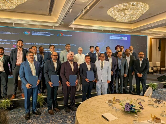
India’s semiconductor ambitions are moving into another phase. At a meeting in New Delhi on November 6, 2026, Union Minister for Electronics and IT Ashwini Vaishnaw launched the SEMICON 2.0 web application portal and announced 12 more approvals under the Electronics Components Manufacturing Scheme (ECMS). Together, the announcements point to a push to build the materials, equipment, and component supply chains needed to support semiconductor manufacturing.
Companies can now apply under three of SEMICON 2.0’s six pillars: semiconductor manufacturing equipment and materials, setting up more fabrication facilities, and assembly, testing, marking and packaging/ outsourced semiconductor assembly and test (ATMP/OSAT).
The portal guides applicants through registration, eligibility checks, and project details, including financial information, technology ownership, partnerships, proposed location, and employment. Applicants can save drafts, track submissions and raise queries with the India Semiconductor Mission team.
Vaishnaw described the government’s approach as a gradual move deeper into the electronics value chain. “The journey was to go straight step by step from finished product to the modules, to the components, to the materials,” he said.
He pointed to progress in battery cells, copper foils and copper-clad laminates as examples. The next challenge, he said, is attracting major equipment manufacturers and suppliers of chemicals and gases. “The first unit is extremely important in chemicals and equipment. We must get the best so that it sets the benchmark for the rest of the industry.”
The approved projects fill important gaps
Twelve applicants received ECMS approval, with proposed investments of ₹75.03 billion, projected production of ₹390.45 billion and an estimated 7,127 direct jobs.
The approvals cover multilayer printed circuit boards (PCBs), relays, heat sinks, specialty ceramics, copper foil, battery anode and cathode materials, capacitor-grade polypropylene film, camera rims and capital goods.
The projects include NeST ICELR’s multilayer PCBs, TDConnex’s relays and precision tooling, Modern Automotives’ heat sinks, and Voltix Semicon’s specialty ceramics. Indo Asia Copper will manufacture copper foil, while TACC and Vidyuta Materials will make battery anode and cathode materials. Enerfolie’s project covers polypropylene film, and Surface Modification Technologies will manufacture camera rims. Rockwell Automation India and Wipro Pari Robotics are among the approved capital goods applicants.
In an interaction with EFY, Ranjit Singh Chugh, CEO of Indo Asia Copper, explained that producing copper foil involves treating both sides of the material. He described the surface treatment process as “pure chemistry”, with technology and equipment support, including process recipe transfer, planned across five grades.
The projects span Gujarat, Karnataka, Madhya Pradesh, Maharashtra, Punjab, Tamil Nadu and Uttar Pradesh. The government said the latest approvals also mark the first ECMS projects in copper foil, cathode active material and specialty ceramics. Vaishnaw noted that nearly half of the approved units are micro, small and medium enterprises (MSMEs), whose role in supplying larger manufacturers will be important to the growth of the ecosystem.
The opportunity extends beyond chipmakers
In an interaction with EFY, a ministry adviser with experience in semiconductor fabrication pointed to a less visible part of the ecosystem: the infrastructure that keeps a fab running.
“If you go to a fab, you will not see any electronics,” he said. Much of the work happens inside enclosed equipment, while chemical and gas lines supply the materials required for wafer processing.
“The difference is only the purity,” he said, comparing India’s existing chemical manufacturing base with the much stricter purity requirements of semiconductor production.
This creates opportunities for suppliers of valves, sensors, monitoring systems, precision pipes and chemical delivery equipment, even if they do not have the resources to build a fab themselves. The industry will also need chemical and mechanical engineers, along with specialists in materials and automation. Training programmes and bridge courses could help prepare them for these roles.
The challenge now is to turn applications and approvals into operating facilities, capable suppliers, and skilled teams. For Indian manufacturers, the opportunity may lie not only in making chips, but also in supplying the systems and materials that keep chip manufacturing running.