


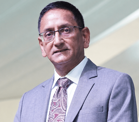

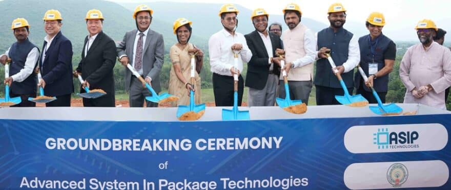
Prime Minister Narendra Modi recently laid the foundation stone for ASIP Technologies’ semiconductor facility in Tarluvada, Visakhapatnam. In an interaction with EFY’s Nitisha Dubey, ASIP Technologies’ Venkata Simhadri discusses the company’s investment allocation, future plans, and the challenge of building a skilled workforce and disciplined manufacturing environment.
Q. What does ASIP Technologies do, and what are its key areas of focus?
A. ASIP Technologies is an Outsourced Semiconductor Assembly and Test (OSAT) company that describes itself as a design-enabled OSAT. We primarily focus on advanced semiconductor packaging, with our initial focus on flip-chip BGA technology.
Q. The project involves an investment of ₹25 billion. How will this investment be deployed across the facility, equipment, and technology?
A. The ₹25 billion investment will be deployed in two stages—Plant 1 and Plant 2. For Plant 1, we are investing more than ₹5 billion, while Plant 2 will involve an investment of more than ₹20 billion. The facility is being built at Tarluvada in Visakhapatnam, where the Andhra Pradesh government has allocated around 30 acres of land. A significant portion of the investment will go towards constructing the factory and cleanrooms, while a major share will also be spent on semiconductor packaging and testing equipment. Most of the equipment will initially be imported.
Q. What will be the initial production capacity, and how do you plan to scale it over the next three to five years?
A. In Phase 1, we are targeting a production capacity of more than 100 million units per year. The facility will operate continuously in three shifts. In Phase 2, we plan to significantly expand capacity, with an eventual target reaching around 300 million units per year.
Q. What packaging and testing technologies will the facility initially support, and how will the technology roadmap evolve?
A. Plant 1 will primarily focus on flip-chip BGA packaging, which is already considered an advanced packaging technology compared with other OSAT capabilities being established in India. In Phase 2, our roadmap is to transition towards more advanced packaging technologies, particularly 2.5D packaging.
Q. What types of semiconductor packages will the Visakhapatnam facility manufacture, and which applications will it initially target?
A. Both technologies are relevant to advanced applications such as data centres, artificial intelligence, high-speed networking, and communications. They are also used for processors in laptops and smartphones, as well as GPUs.
Q. How much of the equipment and technology ecosystem will be domestic, and where will ASIP remain dependent on global suppliers?
A. Most leading equipment suppliers already have distribution and technical-support teams in India, either directly or through local partners. However, the equipment itself will largely come from global suppliers initially. Many multinational suppliers are now considering manufacturing equipment and materials in India. Over the next three to four years, we expect more of these products to become available locally, although they may still be manufactured by multinational companies operating in India.
Q. Will the Visakhapatnam facility primarily serve the Indian market, or will exports also be a part of the strategy?
A. Semiconductor is a global ecosystem, so we cannot build our business purely around the domestic market. We intend to become a global semiconductor manufacturing company headquartered in India and operating globally. Export-oriented manufacturing will therefore be an important part of our strategy.
Q. When do you expect commercial production to begin, and what are the key milestones between the laying of the foundation stone and the start of operations?
A. The first milestone is completing the factory structure, which we expect to take around eight to nine months. This will be followed by equipment installation and trial production, which should take another three months. After that, we will undertake volume-production qualification and certification, which could take another three months. Overall, the timeline could range from 12 to 15 months, with the best-case scenario being around 12 to 13 months. Our target is to enter volume production by Q4 2027.
Q. Who are likely to be the first customers for the facility?
A. In the semiconductor industry, customer names are generally confidential, so we cannot disclose them. However, ASIP Technologies is a joint venture with an established Korean OSAT company, which has agreed to take at least 50% of the capacity of the new plant. We are also in active discussions with two to three other customers who are interested in using capacity from the facility.
Q. When do you expect the facility to break even and become profitable?
A. Within approximately one year of starting production, we expect to reach operational break-even and become profitable. The actual timeline will depend on how efficiently we utilise the capacity. Whether the factory operates at 50%, 80%, or 90% utilisation will significantly impact profitability. We expect to become profitable with positive cash flow by 2028.
Q. What level of automation will be deployed across assembly, inspection, testing and material handling?
A. Once the production line is set up and wafers are fed into it, the process will be highly automated. There will not be people manually performing tasks such as soldering individual chips. However, OSAT facilities handle multiple customers and product types. Whenever we switch from one product to another, machines and processes need to be reconfigured and requalified. Engineering teams will therefore play an important role in product changeovers and process qualification.
Q. What role will AI, machine vision, and data analytics play in the facility?
A. Inspection systems will play an important role in maintaining quality and improving yield. For example, during packaging, inspection systems can determine whether a chip has been properly packaged or connected to the substrate. AI-based inspection and defect-detection applications can help identify issues for improved quality analysis.
Q. What testing capabilities will the plant have? Will it cover wafer-level testing, final testing, burn-in and reliability testing?
A. Yes. The facility is planned to have comprehensive testing capabilities covering the different stages, including wafer-level testing, final testing, burn-in, and reliability testing.
Q. What are the most technically challenging processes that ASIP Technologies expects to establish locally?
A. One of the biggest challenges will be developing the right workforce and establishing the manufacturing discipline required to operate the facility at high efficiency and with low defect density. The initial workforce can be trained in the technical aspects of the job, but running a semiconductor manufacturing facility requires a high level of discipline, consistency, and attention to detail.
Q. What are the biggest gaps in India’s domestic OSAT ecosystem today?
A. The biggest gap is trained talent, particularly people who understand semiconductor packaging and testing technology and know how to operate a factory at very high efficiency. There is also a shortage of experienced semiconductor manufacturing leadership in India. We are looking at bringing in some senior leadership from Asia or Korea to help establish the factory and reach the required efficiency levels during the first one to two years.
Q. How does ASIP Technologies plan to build its workforce?
A. We have already been hiring and training people over the past six months to one year, particularly for testing and manufacturing. For packaging, we have identified the initial engineering team. The first batch of engineers will travel to Korea for training at our partner’s facility. They will then return to India and train additional employees here. Our Korean partner will also deploy engineers in India to help establish the factory, set up the assembly lines, and ensure that the facility operates correctly.
Q. Are you collaborating with academic institutions to develop semiconductor packaging and testing talent?
A. Yes. We have signed MoUs with IIT Hyderabad and IIT Tirupati. Our collaboration with IIT Hyderabad will focus primarily on packaging, including package design and development of new packages. IIT Tirupati will primarily support our testing activities. Testing is as important as manufacturing because we need to ensure that packaged chips meet the required quality standards and that defective chips do not reach customers.
Q. Which materials and components need to be manufactured domestically to make India’s OSAT ecosystem more sustainable?
A. A wide range of materials are required for semiconductor packaging. For wire-bond packaging, for example, the industry uses extremely high-purity wires, including copper wires. For flip-chip packaging, we need substrates, bonding materials, soldering materials, cleaning materials, and other specialised consumables. As semiconductor demand grows in India, multinational suppliers are expected to establish manufacturing operations or joint ventures here. Over the next three to four years, we expect more of these materials to be manufactured and sourced locally.
Q. How will ASIP Technologies manage supply-chain risks for critical equipment and materials?
A. Our Korean partner provides an advantage because it already has established relationships with key component and equipment suppliers. We will leverage these relationships during the initial years and maintain adequate inventory to minimise supply-chain disruptions. The objective is to ensure that we have sufficient material availability during the first one to two years as the facility becomes operational.
Q. Will the Tarluvada facility have a dedicated R&D or process-development centre?
A. We will have a small in-house R&D facility, but our R&D strategy will involve collaboration with multiple institutions and partners. We are working with IIT Hyderabad and IIT Tirupati, and we have also participated in IDSPS, an R&D initiative headed by Prof. Rao Tummala and driven by both the Indian Government and Industry consortium. Our Korean partner also has its own R&D capabilities and technology roadmap. Therefore, our future R&D efforts will be a joint effort involving our internal team, academic institutions, government initiatives, and our Korean partner.
Q. Which areas of semiconductor packaging offer the greatest opportunities for Indian startups and research institutions?
A. On the design side, there is significant opportunity in advanced package design. India already has strong semiconductor design talent, and we are investing in developing capabilities for technologies such as 2.5D packaging. On the manufacturing side, advanced packaging, particularly 2.5D, is an important opportunity. Companies globally are pursuing different approaches; for example, TSMC and Intel have their own advanced packaging technologies. India has an opportunity to develop its own roadmap and technology capabilities in advanced packaging and eventually play a meaningful role in the global market.
Q. What will determine whether a global semiconductor company chooses an Indian OSAT over established facilities in Taiwan, China, Malaysia, and other markets?
A. The first and most important factor is quality. An Indian OSAT has to produce products that meet the same quality standards as established by global players. The second factor is reliability. If a customer needs one million chips within a particular timeframe, we must be able to deliver that volume on time without compromising quality. The third factor is cost competitiveness. Once we achieve the required quality and reliability, we have to become competitive with established OSATs as volumes increase. Government incentives can provide a runway during the initial years, but in the long term, Indian OSATs will have to compete globally on their own merits.
Q. Will the facility support both lead and leadless semiconductor packages?
A. Our initial technology roadmap includes wire-bond and flip-chip BGA packages. The exact mix of lead and leadless packages will depend on customer requirements and the technology roadmap we establish.
Q. Will the facility manufacture plastic packages, ceramic packages, or both?
A. We would like to support as wide a variety of packages as practical, including both types where feasible. However, the exact package mix will depend significantly on our initial customers and their requirements. We are currently focusing our equipment procurement on two to three key areas, based partly on inputs from our Korean OSAT partner regarding market demand and potential capacity that can be moved to India.
Q. How critical are temperature, humidity, vibration, and particulate control to the manufacturing process?
A. All of these parameters are critical. The factory structure must meet specific vibration requirements, particularly for the installation and operation of semiconductor equipment. The cleanrooms must also maintain the required temperature, humidity, and air-particle specifications. These environmental controls are essential for maintaining process stability, quality, and yield.
Q. How much water will the facility consume, and what water treatment and recycling systems are being planned?
A. The Andhra Pradesh government has committed to supplying water to the facility. I do not have the exact annual consumption figure at this stage. We will have our own water-treatment system to purify the water to the required level for manufacturing. The facility will also have a water-recycling system, with most of the water being recycled and reused within the plant or for other purposes.
Q. What level of environmental monitoring will be implemented at the facility?
A. The facility is being developed as a green-certified OSAT facility. We will have the necessary processes and systems in place to maintain the required environmental standards and ensure responsible management of water and other resources.
Q. What is your larger vision for ASIP Technologies once the Visakhapatnam facility becomes operational?
A. Our immediate objective is to establish the facility, achieve stable production, deliver consistent quality to customers and become profitable. Once we have successfully established the first phase, our focus will shift towards Phase 2 and more advanced packaging technologies such as 2.5D packaging. Our long-term objective is to build a globally competitive semiconductor manufacturing company in India that can serve customers not only in India but across the global semiconductor ecosystem.

