
ERS electronic has delivered its first automated 310×310 mm panel-level packaging system to a semiconductor manufacturer, integrating bonding, debonding and detaping to support higher-throughput AI and chiplet packaging.
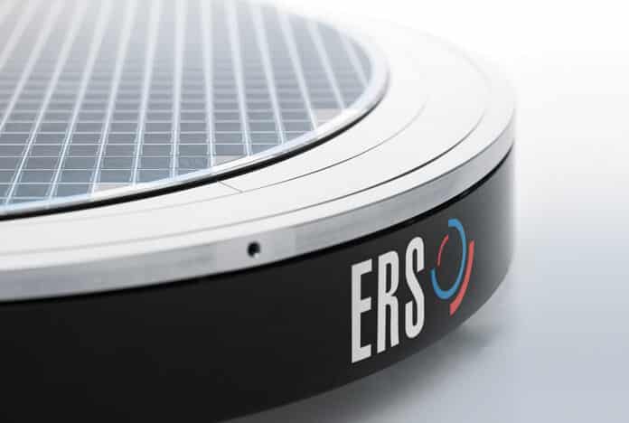
ERS electronic has unveiled a fully automated 310×310 mm panel-level packaging (PLP) system designed for advanced semiconductor packaging applications involving AI and chiplet architectures.
The system integrates temporary carrier bonding, debonding, and detaping into a single automated platform, eliminating panel transfers between separate machines for these thermally critical processes. It can process 13 panels per hour. The first unit has been delivered to a leading semiconductor manufacturer for integration into its panel production line.
The platform supports dual-carrier bonding and debonding workflows for backside processing in 3D IC, HBM, and 2.5D IC packaging. ERS says keeping these processes within one platform can reduce panel handling, transit time, substrate-damage risk, and process variation, without requiring changes to the surrounding fab layout.
The 310×310 mm panel format is gaining traction because it offers significantly better substrate-area utilisation than 300 mm circular wafers. Yole Group projects the panel-level packaging segment to grow at a CAGR of more than 40% over the next five years.
“Our new machine reflects our commitment to solving real manufacturing challenges. By integrating three process steps that have traditionally required separate tools into one automated platform, we’re enabling customers to streamline production, improve process consistency, and achieve higher yield and throughput,” says Laurent Giai-Miniet, CEO, ERS electronic GmbH.
The machine is developed and manufactured at ERS’s Advanced Packaging facility in Barbing, Germany, which combines 55 years of thermal-management expertise with more than 30 years of machine-building capability.