
ERS Launches 310×310mm Packaging System For AI And Chiplet Chips

ERS electronic has delivered its first automated 310×310 mm panel-level packaging system to a semiconductor manufacturer, integrating bonding, debonding and detaping to support higher-throughput AI and chiplet packaging.

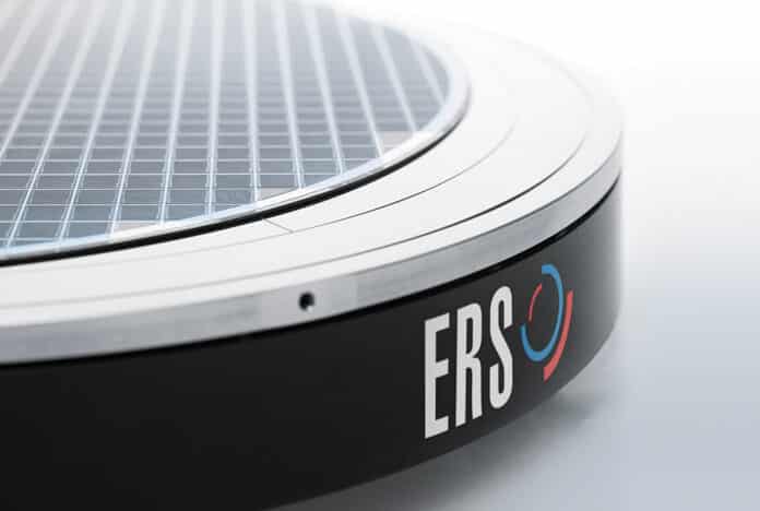
ERS electronic has unveiled a fully automated 310×310 mm panel-level packaging (PLP) system designed for advanced semiconductor packaging applications involving AI and chiplet architectures.

The system integrates temporary carrier bonding, debonding, and detaping into a single automated platform, eliminating panel transfers between separate machines for these thermally critical processes. It can process 13 panels per hour. The first unit has been delivered to a leading semiconductor manufacturer for integration into its panel production line.

The platform supports dual-carrier bonding and debonding workflows for backside processing in 3D IC, HBM, and 2.5D IC packaging. ERS says keeping these processes within one platform can reduce panel handling, transit time, substrate-damage risk, and process variation, without requiring changes to the surrounding fab layout.

The 310×310 mm panel format is gaining traction because it offers significantly better substrate-area utilisation than 300 mm circular wafers. Yole Group projects the panel-level packaging segment to grow at a CAGR of more than 40% over the next five years.

- Advertisement -

“Our new machine reflects our commitment to solving real manufacturing challenges. By integrating three process steps that have traditionally required separate tools into one automated platform, we’re enabling customers to streamline production, improve process consistency, and achieve higher yield and throughput,” says Laurent Giai-Miniet, CEO, ERS electronic GmbH.

The machine is developed and manufactured at ERS’s Advanced Packaging facility in Barbing, Germany, which combines 55 years of thermal-management expertise with more than 30 years of machine-building capability.


- Advertisement -
Loading form…

Industry's Buzz

UST Selects 19 Startups for D3 Startup Challenge 2026 in Bengaluru

0
The programme is designed to identify technologies that address business challenges, assess their practical applications and determine their potential to scale UST, an AI and...
Tonbo Imaging

Tonbo Imaging Launches IPO Driven by Strong Grey Market Demand

0
Bengaluru defence firm targets $102.5 million through pure offer-for-sale IPO as subscription opens.  Bengaluru-based defence technology firm Tonbo Imaging India opened its public offer for...

DigiKey Announces Investment for Distribution Centre Expansion and Automation

0
The announcement follows a period of strong business growth, with DigiKey projecting growth of more than 50% in 2026 DigiKey has announced an investment of...

Japan Funds $21B GlobalFoundries Chip Plants in US

0
The state-of-the-art plants in Malta will boost semiconductor manufacturing through a landmark bilateral trade agreement between the US and Japan.    GlobalFoundries is set to construct...

Thermocool Directs $4.8 Million Towards New Expansion Site

0
The homegrown appliance brand boosts local output and targets new product categories with advanced, AI-driven expansion site.  Indian domestic appliances manufacturer Thermocool Home Appliances has...

Learn From Leaders

Does India’s Chip Packaging Growth Need Local Materials At Scale?

0
What will it take for specialised semiconductor materials manufacturing to grow in India? Packaging volumes will be a key factor as OSAT facilities move...
Ronak Kumar Samantray, Founder, TM2Space Technologies Pvt Ltd.

“Our goal is to build data centres in space.” – Ronak Kumar Samantray, TM2Space

0
A space startup aims to build orbital data centres, letting users run AI models and store data on satellites while also supplying satellite hardware...

India’s Photonics Puzzle Is Finally Coming Together 

0
Can India turn its scattered photonics capabilities into a stronger industry? A new association aims to connect the ecosystem and strengthen the domestic value...
Jin Bains, CEO, Mini-Circuits

Mini-Circuits CEO Jin Bains on Navigating High-Frequency Component SWaP-C Constraints, Emerging Markets, and Career...

0
In this exclusive, Jin Bains, Chief Executive Officer (CEO) of Mini-Circuits, explains in a conversation with Dilin Anand of EFY about areas of emerging...

India Needs Not a Hundred, But Thousands of Chip Diversified Companies 

0
Can India build a semiconductor ecosystem beyond fabs? Indiesemic believes thousands of diversified chip companies are needed to make that possible. India’s semiconductor push is...

Startups

UST Selects 19 Startups for D3 Startup Challenge 2026 in Bengaluru

0
The programme is designed to identify technologies that address business challenges, assess their practical applications and determine their potential to scale UST, an AI and...

Compcarta Reduces The Cost And Complexity Of End-To-End Chip Design

0
Building a chip should not require assembling an entire design ecosystem. A Noida-based startup is developing a browser-based EDA platform that aims to reduce...

Aquaexchange Brings Monitoring And Automation To Shrimp Farming

0
The startup has developed an AI- and IoT-enabled platform that helps shrimp farmers manage farms, access financing, monitor operations, and connect with markets. The startup...

Drone-Like Aircraft For Logistics From BluJ Aerospace

0
Hyderabad-based BluJ Aerospace is developing indigenous electric and hydrogen-powered vertical take-off and landing (VTOL) aircraft for remote cargo transport. BluJ Aerospace, a Hyderabad-based aerospace startup...
Jash Jetly, Co-founder and CEO of EVE

“The cloud isn’t the only way to run AI. We’re proving it can happen...

0
A startup is building a decentralised AI and communication network that runs across everyday devices instead of centralised cloud servers. In an interview, Jash...