
State approves $1.14bn in semiconductor projects spanning silicon carbide fabs, advanced glass substrates, and power electronics.
India has approved 12 semiconductor projects with a total investment of $17.10 billion under the first phase of the India Semiconductor Mission (ISM), two of which are being established in Odisha.
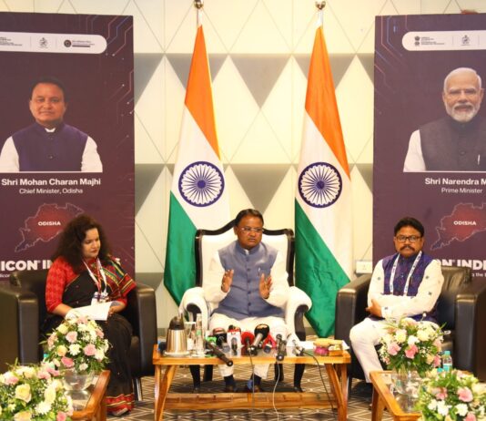
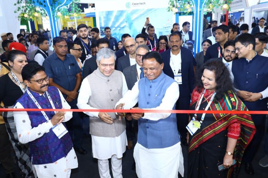
Speaking to the media after inaugurating the Odisha booth at Semicon India 2026, at Yashobhoomi, Dwarka, Chief Minister (CM) of Odisha Mohan Charan Manjhi said that Odisha has become one of the first states to align its semiconductor policy with Semicon 2.0, approved by the Union Cabinet in July 2026.
Odhisa has approved five semiconductor projects with a cumulative investment of $1.14 billion, which are expected to create 4500 direct and more than 16,000 indirect jobs, according to the CM.
The projects cover a vast range of sectors, such as silicon carbide (SiC) manufacturing, glass substrates, advanced packaging, memory module assembly, and power electronics. The components have appications in EVs, railways, defence, energy, and other critical sectors.
Backed by ISM, SiC wafer manufacturer SiCSem Pvt Ltd is establishing a fab integrated with packaging facilities for the first time in India. This could strengthen Odisha’s position in semiconductor manufacturing.
Another major project being established through ISM in Odisha is Heterogeneous Integration Packaging Solutions (HIPS/3DGS), which is setting up an advanced glass substrate packaging facility, described as a technology with applications in artificial intelligence (AI) systems.
In addition to the ISM-supported projects, RIR Power Electronics is going to invest in Odisha in SiC power devices, Sancode Technologies is developing facilities for advanced packaging, and ASP Semicon is setting up memory module OSAT operations. Of these, RIR Power Electronics has already erected a SiC epitaxial wafer manufacturing reactor facility in Bhubaneshwar, the company’s first such facility in India.
Looking ahead, the state plans to utilise the Intel-3DGS MOU to attract investment in advanced glass substrates and advanced packaging. SiCSem’s Phase II is also exploring a SiC and GaN fab and packaging facility.
The government has also approved the ‘National Industry Co-Development Hub on Integrated Power Electronics’ at IIT Bhubaneshwar. The project, under the Indian Design Semiconductors, Packaging and Systems (IDSPS) programme, is jointly funded by the Odisha government, the Ministry of Electronics and Information Technology (MeiTY), the Anusandhan National Research Foundation, and industry partners.
Under its semiconductor policy, the Odisha government will provide 25 per cent state fiscal support on eligible capital expenditure (Capex) for ISM-approved projects. In addition, a silicon valley is planned at Naraj, for which a 871-acre land bank has been created.