Yole Group report predicts 27% compound annual growth as AI hardware architectures push reticle-size limits.
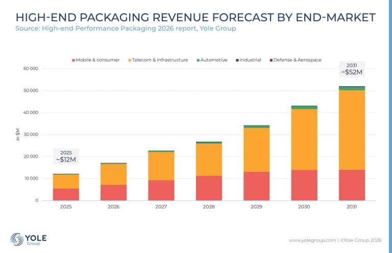
Driven by the rapid adoption of artificial intelligence accelerators, High Bandwidth Memory (HBM) integration, and co-packaged optics (CPO), the global market for high-end performance semiconductor packaging is forecast to exceed $51 billion by 2031, according to market intelligence firm Yole Group.
The sector is projected to expand at a compound annual growth rate (CAGR) of 27 per cent between 2025 and 2031. Package unit volumes will grow by 33 per cent and wafer demand will rise by 30 per cent over the same period.
The divergence across these growth metrics highlights an industry-wide transition toward larger, increasingly complex multi-chiplet architectures designed to bypass physical silicon constraints.
Telecoms and data centre infrastructure will serve as the primary commercial engine, expanding to more than $36 billion by 2031 to account for 70 per cent of total sector revenue.
Mobile and consumer applications remain the second-largest market segment, anchored by client processors from Apple, Huawei, and Intel. Automotive packaging represents the fastest-growing niche at a 36 per cent CAGR due to advanced driver-assistance systems and high-density compute requirements.
On the technical front, mold interposers—such as TSMC’s CoWoS-L format—dominate the 2.5D packaging landscape, growing at a 28.1 per cent CAGR as AI graphics processors and application-specific integrated circuits (ASICs) approach maximum reticle limits.
To overcome these scaling bottlenecks, next-generation packaging formats including CoPoS and CoWoP are scheduled for commercial deployment between 2028 and 2029.
Simultaneously, 3D hybrid bonding for logic and memory is bifurcating into two distinct operational paths. Die-to-wafer technology represents the larger market share, expanding at a 65 per cent CAGR through TSMC’s System-on-Integrated-Chips (SoIC) platform across AMD, Apple, and Nvidia products.
By contrast, wafer-to-wafer integration is scaling rapidly via Huawei’s proprietary LogicFolding architecture manufactured by SMIC.
Furthermore, CPO optical engine packaging is set to scale from a negligible baseline in 2025 to several hundred million dollars by 2031. This marks the arrival of 3D integration—incorporating through-silicon vias (TSVs), microbumps, and direct bonding—within AI data centre networking.
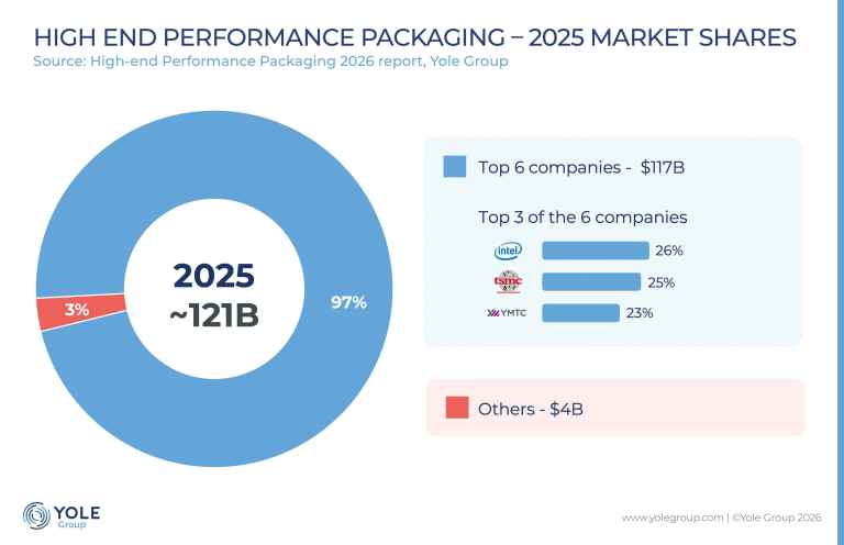
The competitive landscape remains exceptionally concentrated, with the top six suppliers—TSMC, Intel, Samsung, SK Hynix, Micron, and YMTC—capturing approximately 97 per cent of total market revenue in 2025.
TSMC anchors the 2.5D supply chain through its foundries in Taiwan and planned facilities in Arizona. It relies on outsourced semiconductor assembly and test (OSAT) partners such as ASE, Amkor, and Powertech Technology for secondary assembly, while Ajinomoto Build-up Film (ABF) substrates remain a critical upstream bottleneck.
Intel continues to operate a US-centric integrated device manufacturing flow using its Foveros and EMIB silicon bridge technologies. The company is expanding packaging capacity to Malaysia and utilising OSAT partnerships in South Korea to meet surging enterprise demand.