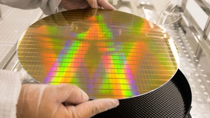

As foundries rethink older production lines, chipmakers face a difficult question: where will they find the capacity to keep existing products running?
Samsung and TSMC are slashing 8-inch wafer capacity, a move that could push utilisation toward 90% by 2026. As foundries rethink older production lines, chipmakers face a difficult question: where will they find the space to keep existing products running? Samsung has reportedly told customers it plans to exit 8-inch foundry manufacturing by the end of 2030. The company is redirecting workforce and equipment investments towards 12-inch wafer processes.
This shift hits power semiconductors, display driver ICs (DDIs), image sensors, power management ICs (PMICs), and microcontrollers (MCUs). In early 2026, Samsung reportedly stopped accepting orders for new 8-inch products. These capacity changes could make it harder for fabless chipmakers to secure production. South Korean foundries DB HiTek and SK Hynix are already heavily committed to existing customers. Taiwanese foundries have limited spare capacity. Moving production to 12-inch wafers increases costs. It requires chip redesigns and renewed qualification, particularly for analogue chips.
According to TrendForce, capacity cuts by Samsung and TSMC, alongside growing demand for AI-related power chips, could push average 8-inch utilisation among the world’s top 10 foundries to nearly 90% in 2026. That’s up from around 80% in 2025. Utilisation is expected to remain above 80% through the first half of 2027 as global capacity continues to shrink. Separately, TSMC reportedly plans to transfer about 80% of its annual 8-inch wafer capacity—about five million wafers—to its affiliate, Vanguard International Semiconductor, in phases over the coming years.