High-End Semiconductor Packaging Market to Surpass $51bn by 2031

Yole Group report predicts 27% compound annual growth as AI hardware architectures push reticle-size limits.
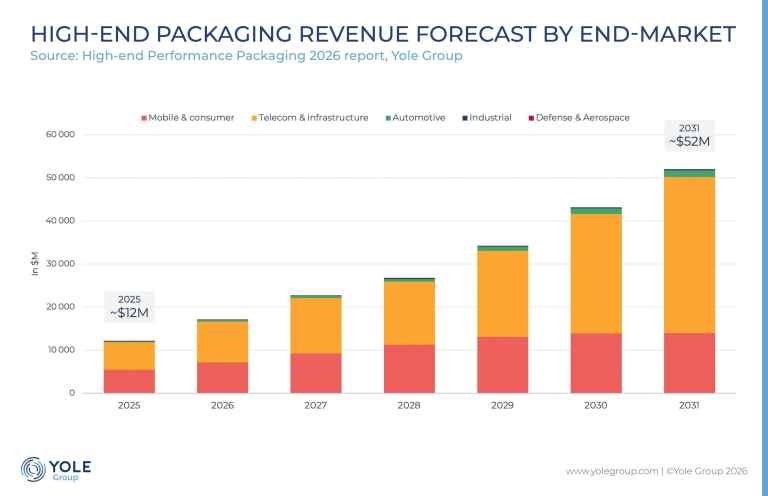
High-End Packaging Market Forecast; Source: Yole Group

Driven by the rapid adoption of artificial intelligence accelerators, High Bandwidth Memory (HBM) integration, and co-packaged optics (CPO), the global market for high-end performance semiconductor packaging is forecast to exceed $51 billion by 2031, according to market intelligence firm Yole Group.

The sector is projected to expand at a compound annual growth rate (CAGR) of 27 per cent between 2025 and 2031. Package unit volumes will grow by 33 per cent and wafer demand will rise by 30 per cent over the same period.

The divergence across these growth metrics highlights an industry-wide transition toward larger, increasingly complex multi-chiplet architectures designed to bypass physical silicon constraints.

Telecoms and data centre infrastructure will serve as the primary commercial engine, expanding to more than $36 billion by 2031 to account for 70 per cent of total sector revenue.

- Advertisement -

Mobile and consumer applications remain the second-largest market segment, anchored by client processors from Apple, Huawei, and Intel. Automotive packaging represents the fastest-growing niche at a 36 per cent CAGR due to advanced driver-assistance systems and high-density compute requirements.

On the technical front, mold interposers—such as TSMC’s CoWoS-L format—dominate the 2.5D packaging landscape, growing at a 28.1 per cent CAGR as AI graphics processors and application-specific integrated circuits (ASICs) approach maximum reticle limits.

To overcome these scaling bottlenecks, next-generation packaging formats including CoPoS and CoWoP are scheduled for commercial deployment between 2028 and 2029.

Simultaneously, 3D hybrid bonding for logic and memory is bifurcating into two distinct operational paths. Die-to-wafer technology represents the larger market share, expanding at a 65 per cent CAGR through TSMC’s System-on-Integrated-Chips (SoIC) platform across AMD, Apple, and Nvidia products.

By contrast, wafer-to-wafer integration is scaling rapidly via Huawei’s proprietary LogicFolding architecture manufactured by SMIC.

Furthermore, CPO optical engine packaging is set to scale from a negligible baseline in 2025 to several hundred million dollars by 2031. This marks the arrival of 3D integration—incorporating through-silicon vias (TSVs), microbumps, and direct bonding—within AI data centre networking.
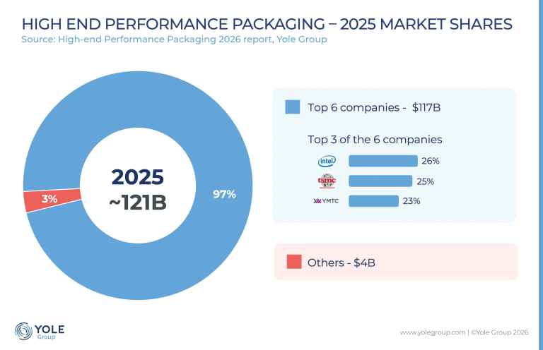
Market Share of Major Players in the High-End Packaging Sector; Source: Yole Group

The competitive landscape remains exceptionally concentrated, with the top six suppliers—TSMC, Intel, Samsung, SK Hynix, Micron, and YMTC—capturing approximately 97 per cent of total market revenue in 2025.

TSMC anchors the 2.5D supply chain through its foundries in Taiwan and planned facilities in Arizona. It relies on outsourced semiconductor assembly and test (OSAT) partners such as ASE, Amkor, and Powertech Technology for secondary assembly, while Ajinomoto Build-up Film (ABF) substrates remain a critical upstream bottleneck.

Intel continues to operate a US-centric integrated device manufacturing flow using its Foveros and EMIB silicon bridge technologies. The company is expanding packaging capacity to Malaysia and utilising OSAT partnerships in South Korea to meet surging enterprise demand.


- Advertisement -
Loading form…
Jaydeep Gadhavi
Jaydeep Gadhavi
Jaydeep Gadhavi is a journalist with EFY business focusing on EV as well as Semiconductor business news.

Industry's Buzz

India Launches Plan for Indigenous Power Grid Semiconductors

0
Ministries issue consultation for domestic SiC MOSFET power modules with guaranteed initial order of 13,000 units. The Indian government has initiated stakeholder consultations to develop...

Electric Mining Fleet Market Set to Exceed $27bn by 2047

0
IDTechEx report predicts rapid adoption of heavy electric machinery driven by total cost of ownership advantages and mega-battery technology. The global market for electric mining...

NUS partners Applied Materials, Micron to build Singapore semiconductor talent pipeline

0
Available on both full-time and part-time bases, the programme covers the semiconductor value chain The National University of Singapore (NUS) has partnered with Applied Materials...
NX Technologies

NX Technologies To Develop Compact Traction Inverters For Light EVs

0
Spain-based NX Technologies has secured €1.9 million in PERTE funding to develop compact traction inverters for light EVs, expanding its European power-electronics portfolio across...
Bentley

Bentley Invests 350 Million Pounds To Build First Electric Car In UK

0
Bentley will invest £350 million at its Crewe headquarters to build the Torcal, its first fully electric vehicle, strengthening UK-based EV manufacturing and its...

Learn From Leaders

Does India’s Chip Packaging Growth Need Local Materials At Scale?

0
What will it take for specialised semiconductor materials manufacturing to grow in India? Packaging volumes will be a key factor as OSAT facilities move...
Ronak Kumar Samantray, Founder, TM2Space Technologies Pvt Ltd.

“Our goal is to build data centres in space.” – Ronak Kumar Samantray, TM2Space

0
A space startup aims to build orbital data centres, letting users run AI models and store data on satellites while also supplying satellite hardware...

India’s Photonics Puzzle Is Finally Coming Together 

0
Can India turn its scattered photonics capabilities into a stronger industry? A new association aims to connect the ecosystem and strengthen the domestic value...
Jin Bains, CEO, Mini-Circuits

Mini-Circuits CEO Jin Bains on Navigating High-Frequency Component SWaP-C Constraints, Emerging Markets, and Career...

0
In this exclusive, Jin Bains, Chief Executive Officer (CEO) of Mini-Circuits, explains in a conversation with Dilin Anand of EFY about areas of emerging...

India Needs Not a Hundred, But Thousands of Chip Diversified Companies 

0
Can India build a semiconductor ecosystem beyond fabs? Indiesemic believes thousands of diversified chip companies are needed to make that possible. India’s semiconductor push is...

Startups

Seema Johar, Co-Founder and Product Director, Compcarta Solutions Pvt Ltd

“We Let Designers Focus on Innovation, Not Infrastructure.”- Seema Johar, Compcarta Solutions

0
In an exclusive interview, Seema Johar of Compcarta speaks with EFY’s Akanksha Sondhi Gaur about why setting up an EDA environment can be harder...

Space Solar Secures $1.7m ARIA Contract for Wireless Power Beaming

0
Harwell-based firm to develop ground-to-air RF beaming technology for persistent high-altitude platforms. Harwell-based wireless power specialist Space Solar has secured a $1.7 million (£1.3 million)...
Mohit Gupta, Founder and CEO, TYLsemi

“We are democratising custom silicon with reusable chiplets, enabling more companies to build their...

0
In an exclusive interview,Mohit Gupta from TYLsemi explains to Saba Aafreen from Electronics For You as to why the future of AI infrastructure will...
Venkata Simhadri, Managing Director and CEO of ASIP

“Running A Semiconductor Manufacturing Facility Requires A High Level Of Discipline, Consistency, And Attention”-...

0
Prime Minister Narendra Modi recently laid the foundation stone for ASIP Technologies’ semiconductor facility in Tarluvada, Visakhapatnam. In an interaction with EFY’s Nitisha Dubey,...
Sarah Osentoski is the Chief Technology Officer of Vinci

A Startup Building An AI Copilot For Physics 

0
What if engineers could solve complex design problems in minutes instead of hours? An AI startup is building a system that uses physics-based AI...