


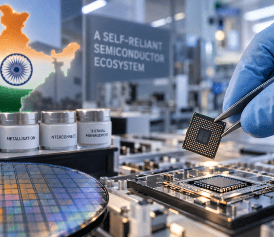

What will it take for specialised semiconductor materials manufacturing to grow in India? Packaging volumes will be a key factor as OSAT facilities move towards production.
MacDermid Alpha Electronics Solutions showcased semiconductor assembly and packaging materials at SEMICON India 2026, spanning die attach, wafer-level packaging, metallisation, interconnect, thermal management, and protection. The company also demonstrated its ATROX CD 560-1 conductive die attach material, which uses a silver-coated copper filler as an alternative to conventional silver-filled materials.
However, the larger consideration for specialised material suppliers is how quickly India’s growing semiconductor packaging capacity translates into sustained production volumes. In an exclusive interaction with EFY, Sharan Aiyappa, sales director, MacDermid Alpha, said the company is seeing more than 10 outsourced semiconductor assembly and test (OSAT) and semiconductor packaging projects being established or planned in India. Yet, current volumes are not sufficient for specialised material suppliers to justify deeper local manufacturing.
According to Aiyappa, the market needs to mature before suppliers can consider dedicated manufacturing for materials used in semiconductor assembly and packaging. This makes production scale an important factor in India’s materials localisation. Packaging facilities can establish capacity, but suppliers also need predictable demand across applications such as die attach, wafer-level packaging, metallisation and interconnect before making manufacturing investments.
MacDermid Alpha already has a long-standing presence in India, but Aiyappa said semiconductor materials require a different level of market scale and qualification. He expects India’s position to look significantly different as the semiconductor ecosystem develops towards 2030.
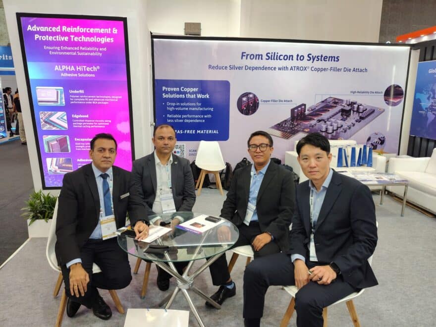
The materials challenge is also evolving alongside package technology. Yil Hak Lee, product manager for wafer-level packaging, pointed to the difficulty of maintaining uniformity as semiconductor dimensions and interconnect structures shrink. The company is also developing metallisation approaches to limit unwanted intermetallic compound formation. Mohamad Syah, who handles standard die attach materials for South Asia, highlighted the need to balance reliability and cost, including reducing exposure to silver price volatility.
For India’s semiconductor packaging ecosystem, therefore, the next step in materials localisation could depend on the transition from setting up facilities to building sustained package production.
What production volumes would make local manufacturing viable, and what would suppliers need to see before taking that step? In a longer interaction, Aiyappa, Syah and Lee discussed the material requirements, market conditions and production scale they are watching for as India’s semiconductor packaging ecosystem develops.

