


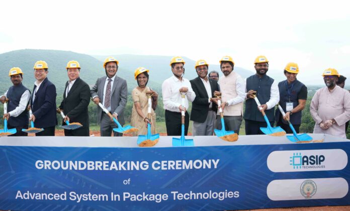

Automation and human expertise are expected to play central roles in the new facility coming up near Visakhapatnam.
ASIP Technologies has commenced work on its ₹25 billion semiconductor packaging and testing facility in Tarluvada, Visakhapatnam, following the virtual foundation stone laying by Prime Minister Narendra Modi. Being developed in two phases, the facility is planned to start with an annual capacity of more than 100 million units before scaling up to around 300 million units in the second phase.
In an exclusive interaction with Electronics For You, Venkata Simhadri, managing director and CEO, ASIP Technologies, revealed that more than ₹5 billion of the investment will be deployed in plant 1, while plant 2 will account for more than ₹20 billion. The Andhra Pradesh government has allocated around 30 acres (121406sqm) for the project at Tarluvada.
A substantial portion of the investment will go towards factory construction, cleanrooms and supporting infrastructure, while advanced semiconductor packaging and testing equipment will constitute another major component of the project. Most of the equipment required during the initial phase is expected to be imported.
The first phase will focus on flip-chip ball grid array (BGA) packaging, with the facility designed to operate round the clock across three shifts. ASIP expects to achieve more than 100 million units of annual capacity in this phase before significantly expanding production in phase 2.
“The initial focus will be flip-chip BGA, while the company’s longer-term roadmap includes 2.5D packaging for applications such as AI, data centres, high-speed networking, communications, processors and GPUs,” said Venkata.
The company expects the facility to become operational within approximately 12–15 months. According to Venkata, construction of the factory is expected to take around eight to nine months, followed by equipment installation and trial production. Volume-production qualification and certification will require additional time. In the best-case scenario, ASIP expects the facility to be ready within 12–13 months, with commercial volume production targeted for Q4 2027.
ASIP has also secured an important anchor for its initial production through a partnership with an established Korean outsourced semiconductor assembly and test (OSAT) company. The partner has committed to taking at least 50 per cent of the facility’s capacity, giving ASIP a significant customer base as it begins commercial operations. The company is also in discussions with two to three additional customers, although their identities remain confidential.
The Korean partner will play a broader role beyond capacity utilisation, supporting ASIP in setting up production lines, training employees and bringing the facility up to the required operational standards. ASIP’s initial engineering team will travel to Korea for training at the partner’s facility before returning to India to train additional employees. Experienced engineers from the Korean company are also expected to be deployed in India during the initial phase.
Venkata identified the availability of trained semiconductor packaging and testing professionals and the need to develop manufacturing discipline as some of the key gaps in India’s emerging OSAT ecosystem. To address these challenges, ASIP has already started hiring and training its workforce and is building academic partnerships to strengthen both talent and technology capabilities.
The company has signed MoUs with IIT Hyderabad and IIT Tirupati as part of this effort. IIT Hyderabad will support packaging and package development, while IIT Tirupati will contribute to semiconductor testing capabilities.
Automation is expected to play a central role in the new facility. Once wafers enter the manufacturing line, a significant portion of the production process will be automated. Engineering teams, however, will continue to be critical for product changeovers, process reconfiguration, troubleshooting and qualification.
ASIP also plans to deploy AI-based inspection, machine vision and automated defect detection systems to improve manufacturing quality and yield. The facility is being designed to offer a broad range of testing capabilities, including wafer-level testing, final testing, burn-in and reliability testing.
While flip-chip BGA will form the technological foundation of Plant 1, ASIP intends to move into more advanced packaging technologies as it expands. The company’s Phase 2 roadmap includes 2.5D packaging, which is increasingly being adopted for high-performance computing and applications involving AI, data centres, processors, GPUs and high-speed communications.
India has an opportunity to develop its own advanced semiconductor packaging roadmap rather than limiting its OSAT ambitions to conventional packaging technologies, emphasised Venkata. The company intends to build capabilities that can eventually compete with established semiconductor manufacturing hubs globally.
ASIP’s strategy is also not limited to serving the Indian market. “Semiconductor is a global ecosystem,” said Venkata, explaining that the company aims to build a global semiconductor manufacturing business headquartered in India and serving customers worldwide.
This global focus will also expose Indian OSAT companies to intense competition from established manufacturing hubs. According to Venkata, Indian semiconductor packaging companies will ultimately need to compete on quality, reliability and cost.
“Government incentives can provide a runway during the initial years, but in the long term, Indian OSATs will have to compete globally on their own merits,” said Simhadri.
ASIP expects the Visakhapatnam facility to reach operational break-even approximately one year after commercial production begins and is targeting profitability and positive cash flow by 2028.
With a ₹25 billion investment, an eventual annual capacity of around 300 million units and a roadmap extending from flip-chip BGA to 2.5D packaging, ASIP Technologies is positioning its Visakhapatnam facility as a major base for advanced semiconductor packaging and testing, with ambitions extending well beyond the Indian market.

