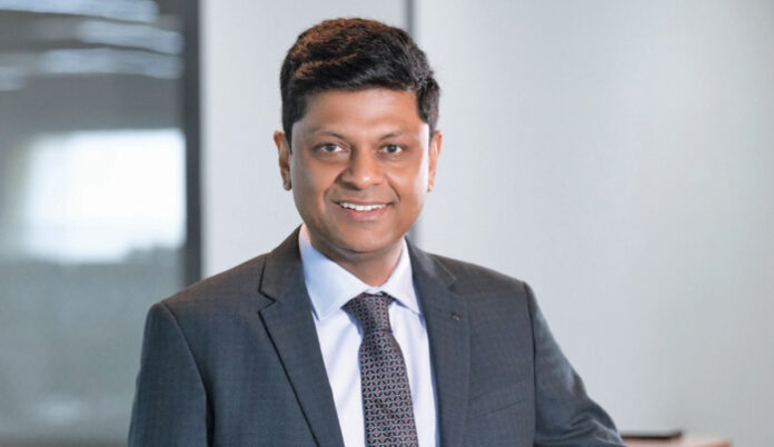

Axiro Semiconductor designs RF and satellite chips, ships millions worldwide, and retains its startup mindset while tackling complex technical challenges. In a conversation with Nidhi Agarwal from EFY, Dr Naveen Yanduru shared insights into the company’s global operations, RF front-end innovations, and what India needs to build and scale its own chip products.
Q. What gaps in satellite infrastructure do you think are still not fully addressed?
A. When it comes to satellite communication, there are three main challenges. First is the G/T, or signal-to-noise performance. Since satellites are far from Earth, systems require very low noise levels to maintain reliable connections, especially given the high path loss. Second is power consumption. Satellite terminals often use large arrays, and if power is not managed effectively, the panels can overheat, and performance can drop. This is especially critical in remote areas with limited access to power. Third is cost. Phased-array systems use many chips, so keeping the overall terminal affordable is key to making services such as LEO constellations commercially viable. These three factors—G/T, power consumption, and cost—are central to the design of competitive satellite communication chips.
Q. How do you handle Doppler shift and fast-moving satellite links at the silicon level?
A. Doppler shift is a critical challenge, especially as video data traffic increases. In traditional systems, analogue beamformers with phase shifters using true-time delays were used, which can address some Doppler-related issues. Implementing true-time-delay-based phase shifting at the silicon level helps, but it increases terminal cost and size because these components are bulkier and more difficult to design. At the system level, customers also apply techniques to mitigate Doppler effects when communicating with fast-moving satellites.
Q. What are the key technical challenges in building up-down converter chips for satellite links?
A. Up-down converters are critical because they handle frequency translation, but this comes with several technical challenges. One major issue is managing spurious signals and out-of-band noise to avoid interference in the transmitter. Another challenge is keeping the intermediate frequency low enough for downstream chips to process it efficiently. However, this brings the image frequency closer, making filtering more difficult. Overall, maintaining low spurious levels, good phase-noise performance, and strong image rejection are the key challenges in designing these chips.
Q. What do you think are the biggest technical bottlenecks in the RF industry?
A. The RF market is broad; anytime wireless communication is involved, RF technology is required. There are opportunities across satellite communications, cellular networks, wireless infrastructure, handsets, and other applications. The main challenge right now is on the cellular side. While 5G deployments are ongoing, 6G still feels like a distant goal, and the industry has yet to develop a compelling business case for it. That makes it difficult to move to the next wave before the current one matures. However, RF spans so many applications that companies can focus on other markets, such as defence and aerospace, to balance short-term slowdowns in the cellular sector.
Q. What are the biggest technical challenges in designing chips for 5G, 6G, and beyond?
A. One of the biggest challenges is the power amplifier. It sits at the antenna and transmits signals that devices such as mobile phones receive. For 5G and future 6G systems, higher-order modulation schemes lead to very high peak-to-average power ratios, making linearity extremely important. Power amplifiers must also be compatible with digital pre-distortion (DPD), enabling systems to maintain both efficiency and gain while meeting error vector magnitude (EVM) and adjacent channel leakage ratio (ACLR) targets. While components such as low-noise amplifiers, switches, and digital step attenuators are also important, the power amplifier has the greatest influence on overall RF front-end performance in modern wireless infrastructure.
Q. What changes do you expect in RF front-end architecture as networks move towards 6G?
A. We expect significantly greater integration in RF front ends. As networks move to higher frequencies such as FR3, the number of radio elements will continue to increase. Currently, massive MIMO systems use 32×32 or 64×64 transmit-receive configurations, but in 6G, 128×128 and even 256×256 systems are likely to become commonplace. Managing such large numbers of elements efficiently will require greater integration, making it a defining trend in 6G RF front-end design.
Q. In Wi-Fi front-end modules, how do you manage coexistence and interference, especially in dense enterprise deployments?
A. Wireless spectrum is becoming increasingly crowded, and interference is a major concern, particularly with adjacent bands such as CBRS and C-band. To address this, we focus on highly linear components with high compression points that are resilient to interference. For example, our Zero Distortion technology ensures that amplifiers and mixers introduce minimal distortion, preventing spurious signals from spilling into adjacent bands. We also use Kalen technology, which maintains linearity (IP3) consistently even as output power changes, and Flat Noise technology, which keeps receiver noise constant even when gain is reduced. Together, these innovations help our modules deliver superior coexistence and interference-mitigation performance compared with competitors.
Q. What do you see as the next big opportunity in wireless or satellite silicon?
A. There are many opportunities, but it is crucial to ensure that technology remains current and that product roadmaps align with market growth. We are focusing on RF transceivers, particularly as the available frequency spectrum expands and the number of elements grows across satellite and wireless infrastructure systems, including hybrid and fully digital beamforming architectures. Another key area is power amplifiers, particularly improving the efficient handling of load modulation and linearisation. Companies that excel in these areas are likely to lead the next generation of communication systems.
Q. What are the biggest barriers Indian semiconductor startups face in scaling up?
A. Investment is a major barrier. Building a strong semiconductor company such as Axiro requires millions—sometimes tens of millions—of rupees before generating even the first rupee of revenue. This high upfront cost often discourages investors. India has significant talent in this area, but much of it is employed by established MNCs such as Qualcomm. Starting from scratch is difficult because the investment requirements are substantial, the risks are high, and the time needed to generate returns is long. Government support exists, and initiatives such as ISM 2.0 can provide semiconductor and product companies with a launchpad for growth. Once three or four successful companies emerge, investment and resources are likely to flow more freely. Currently, the lack of proven success stories is one reason investment in semiconductor startups in India has not scaled significantly.
Q. What technical and infrastructure gaps need to be addressed to make India a competitive semiconductor IP nation?
A. I believe India already has the tools required to succeed in this space. The country has highly talented engineers with strong communication skills and extensive global connectivity. Government support is also increasing, meaning the fundamentals are already in place. Many leading semiconductor companies, such as Qualcomm, Broadcom, Nvidia, and AMD, are led by Indian engineers. Indian talent forms the backbone of these organisations, whether in India, the US, or European design centres, helping deliver cutting-edge products. We already possess the IP and the talent. The primary challenge now is investment, ensuring that more Indian-led semiconductor companies such as Axiro can be created and scaled. The talent is present, the intent is clear, and government support exists. Solving the investment puzzle is the final piece required to accelerate India’s semiconductor IP ambitions.